
PCB Assessment Case
Air Mattress Pump Charging Board Repair
Assessment of a rechargeable air-mattress pump board with reported charging failure and heat damage near the DC input.
Board typeCharging and power-control board
ApplicationPower and Charging
ServiceCharging Board Repair
Fault Description
"I have a rechargeable pump for an air mattress that the circuit board which the charging cable connects into looks like it has been fried."
Diagnosis & Repair Process
The customer reported that the circuit board connected to the charging cable appeared burned and that the rechargeable pump no longer charged normally.
The concern is concentrated around the DC input and nearby power-control section. Visible heat damage can involve the connector joint, input trace, switching device, inductor, protection parts, or damaged board laminate. Below is the complete process covering inspection, repair, testing, and final confirmation.
Phase 1: Inspection and Fault Confirmation
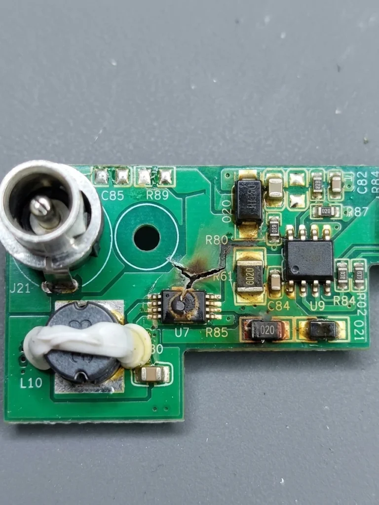
Inspection Report: We inspected the circuit board under a microscope at high magnification, focusing on the main power input traces.
Faults Identified (Figure 1):
-
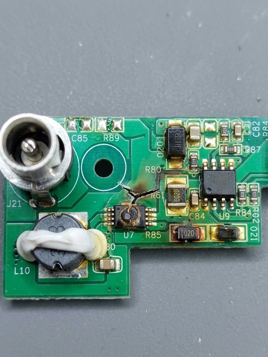
Burned Power Trace: The main positive power trace running from the DC jack positive pin (below C85 and R89) to the power input of U7 was physically broken and severely carbonized. Charger overvoltage or an internal short circuit likely caused high current that burned the trace.
-
Component Damage: The surface of chip U7 (a SOIC-8 power IC, likely an LDO or buck converter) showed discoloration, indicating thermal damage from overheating.
Figure 1 Description:
-
Figure 1: Primary fault detected. Microscope close-up shows a clear break and burn marks on the main power trace between the DC jack (left) and chip U7 (right). Chip U7 also shows surface discoloration.
Phase 2: Repair Action
Repair Plan: Because the main power trace was completely broken, simple component replacement could not fix the board. We needed to repair the PCB substrate and trace damage by installing a jumper wire to rebuild the circuit.
Execution Steps (Figures 2 and 3):
-
Component Removal (Figure 2): Removed the damaged chip U7 and inductor L10 using a hot air station and desoldering braid.
-
Cleaning and Preparation: Cleaned the solder pads and surrounding carbonized substrate to expose clean copper and prepare connection points for the jumper wire.
-
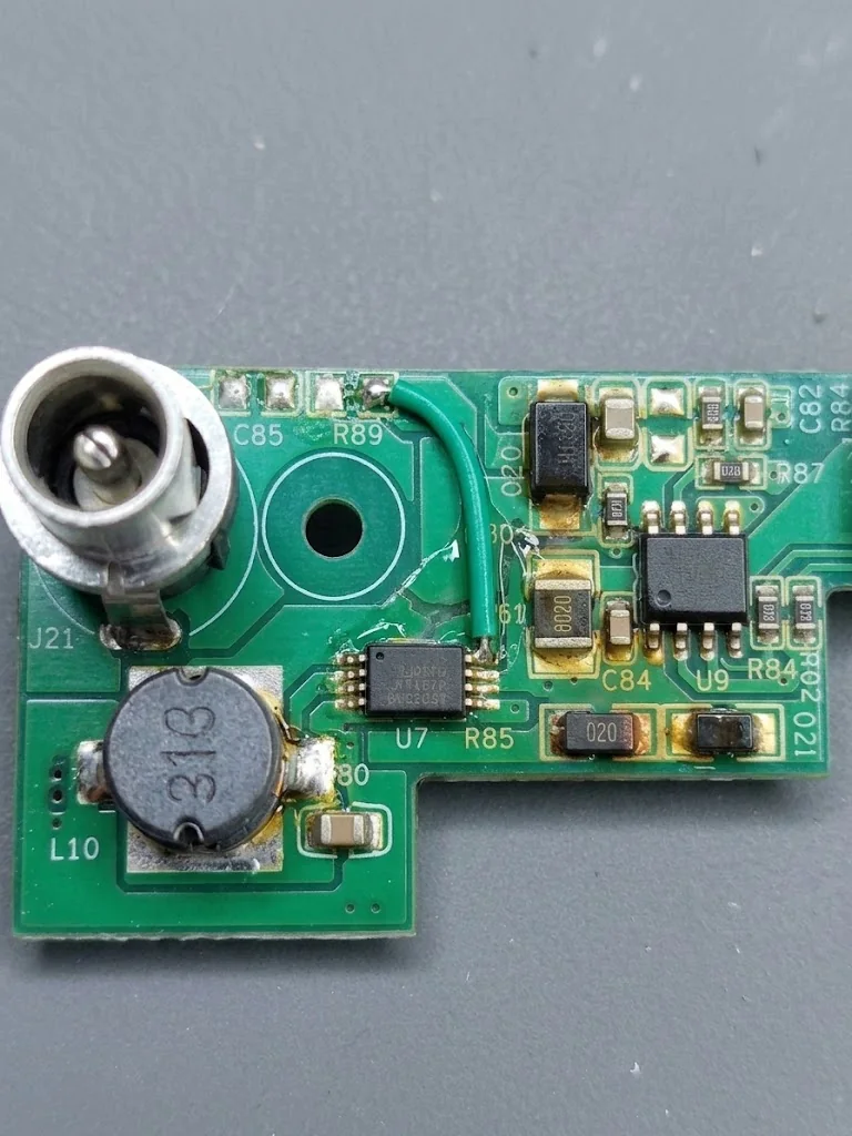
Component Replacement (Figure 3): Installed a new power IC (U7) and a new inductor (L10).
-
Jumper Wire Reconstruction (Figure 3): Because the original trace was ruined, we soldered a fine green jumper wire from a clean test pad (near C85/R89) directly to the input pin of the new U7. This completely bypassed the burned area.
-
Protective Coating (Figure 3): Applied a small amount of clear conformal coating over the jumper wire and sensitive connection points, then cured it with UV light to improve mechanical strength and electrical insulation.
Figure Descriptions:
Figure 2: Component removal. Shows damaged U7 and L10 removed, pads cleaned, and burned FR4 substrate exposed.
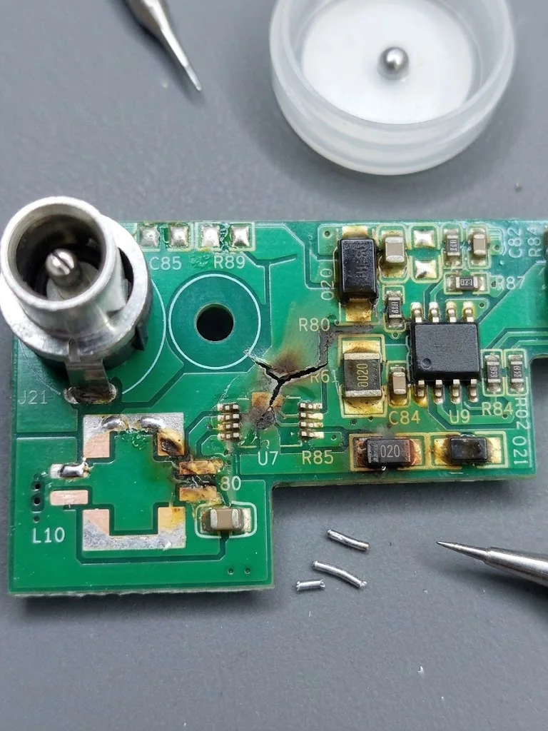
Figure 3: Complete repair. New components (U7 and L10) installed. A fine green jumper wire bypasses the burned area to connect power to the U7 input pin, sealed with clear conformal coating.
Phase 3: Testing Log
Test Plan: After rebuilding the power circuit, we performed a logic-level power-on test.
Test Steps:
-
Connected a 5V DC power supply (current limited to 1A) to the DC input jack.
-
Measured key test points using a digital multimeter (DMM).
Test Results (Figure 4):
-
Input Voltage: 5.02 V DC (measured at the DC jack pads).
-
Output Voltage: 5.02 V DC measured at the U7 output test point (‘TP_OUT’). This confirms that the power management IC works properly, the jumper wire connection is successful, and there are no downstream short circuits.
Phase 4: Final Result
Final Confirmation (Figure 4): The repaired board is clean, solder joints are solid, and the jumper wire is secure and well insulated. The board passed all functional tests.
Conclusion: The inflatable mattress charging pump circuit board has been successfully repaired. It is ready to be reinstalled into the pump unit for normal use.
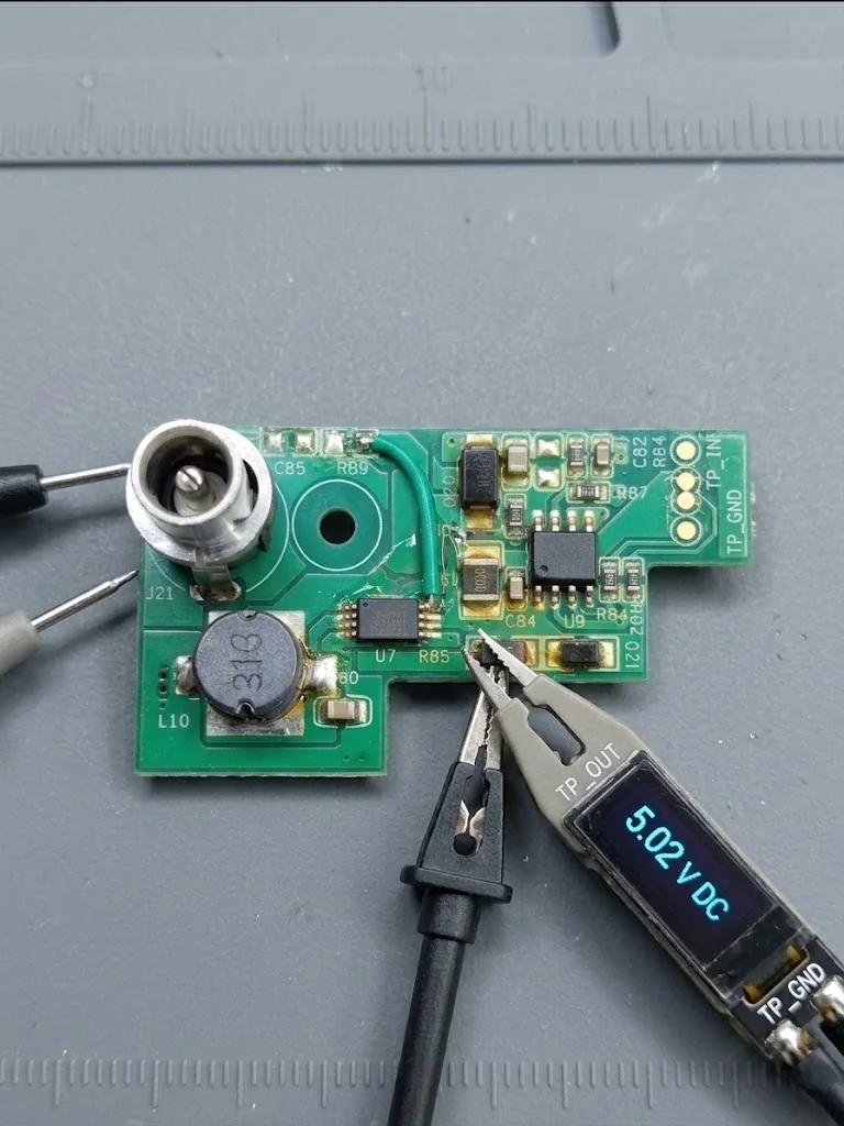
Figure 4 Description:
Figure 4: Final test and results. Full view of the cleaned circuit board. A test probe with a digital display (labeled TP_OUT and TP_GND) connects to the board, showing a clean output of 5.02 V DC.
Related Case
Power and Charging · Power PCB Repair
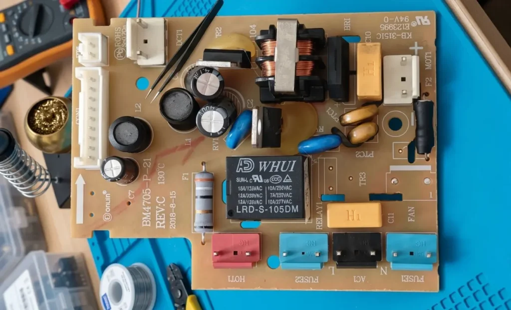
Donlim Bread Maker Power Board (BM4705-P-21) Repair
Fix intermittent motor shutdown on the Donlim bread maker power board (BM4705-P-21) with this step-by-step diagnostic and relay replacement guide.
View case study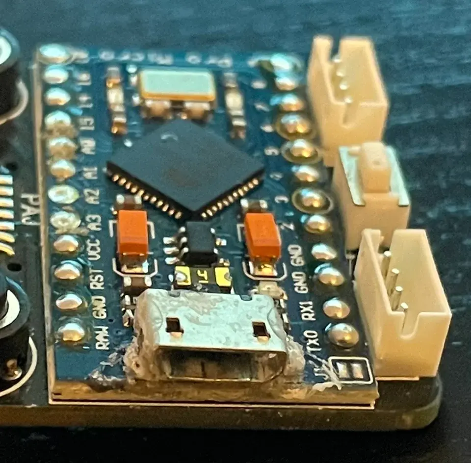
Consumer Electronics · Trace and Pad Repair
Pro Micro USB Port Repair and Trace Bridge
Fix a loose Micro USB port and broken traces on the Pro Micro board with this step-by-step micro-soldering and trace bridging guide.
View case study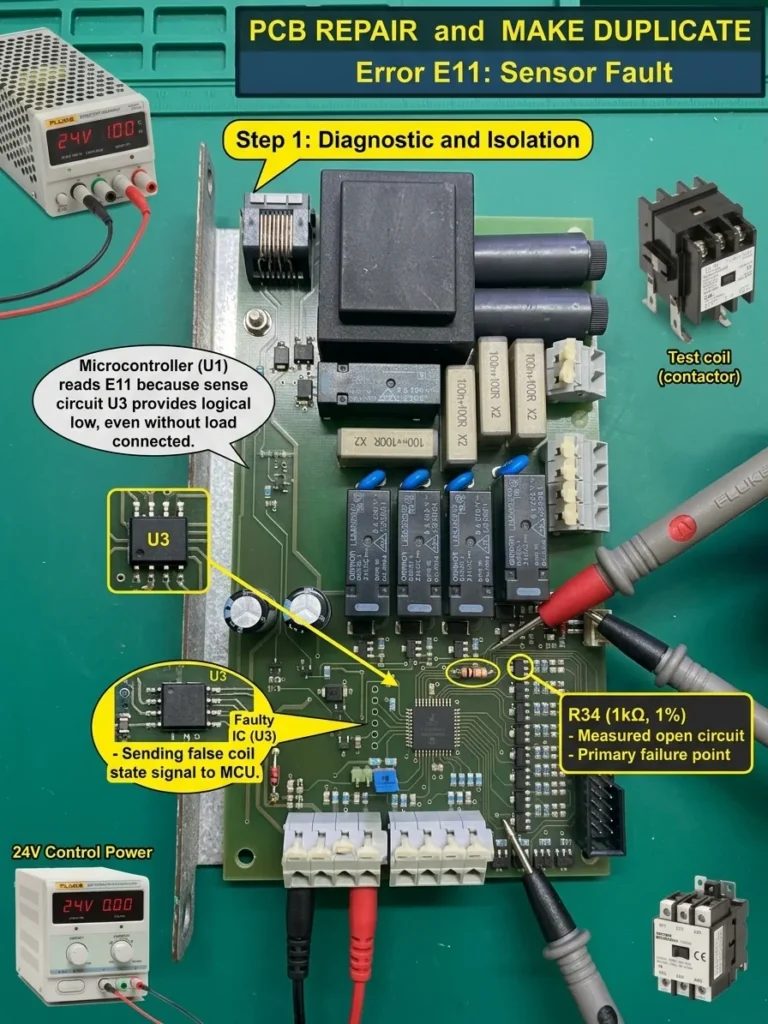
Industrial Control · Control Board Assessment
E11 Relay Control Board Assessment and Repair Planning
Assessment plan for a relay control board reporting E11 ‘coil not working’ even when the external coil is not connected.
View case study
Automotive Service Equipment · Short-Circuit Diagnosis
3D Wheel Alignment Camera Board Short-Circuit Repair
Board-level assessment plan for a short-circuited 5MP camera module from an SM-V2 3D wheel-alignment system.
View case studyDiscuss your board